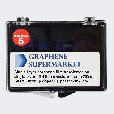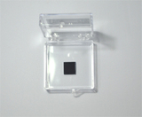


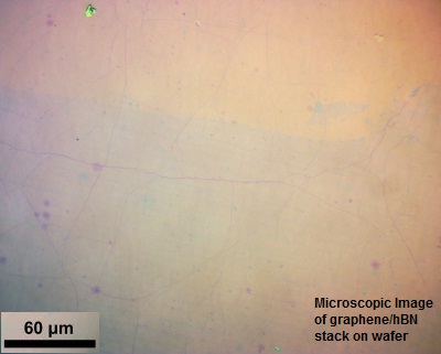
CVD Graphene/CVD Hexagonal Boron Nitride heterostructure on SiO2/Si wafer
Properties of Graphene/h-BN Film:
Single Layer Graphene Film on Single Layer h-BN Film transferred onto 285 nm (p-doped) SiO2/Si wafer
Size: 1cmx1cm; 4 pack
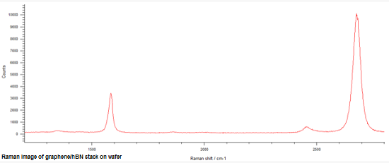
The thickness and quality of each film is controlled by Raman Spectroscopy
The coverage of this product is about 98%
The films are continuous, with minor holes and organic residues
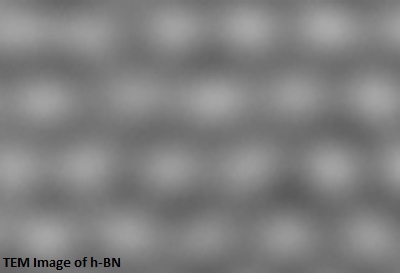
High Crystalline Quality
The graphene film is premodominantly single layer (more than 95%) with occasional small multilayer islands (less than 5% bi-layers)
Sheet Resistance: 430-800 Ω/square
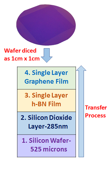
Properties of Silicon/Silicon Dioxide Wafers:
Oxide Thickness: 285 nm
Oxide Thickness: 285 nm
Color: Violet
Wafer thickness: 525 micron
Resistivity: 0.001-0.005 ohm-cm
Type/Dopant: P/Boron
Orientation: <100>
Front Surface: Polished
Back Surface: Etched