歡迎光臨~泰州巨納新能源有限公司
語言選擇:
 ∷
∷

∷
 ∷
∷
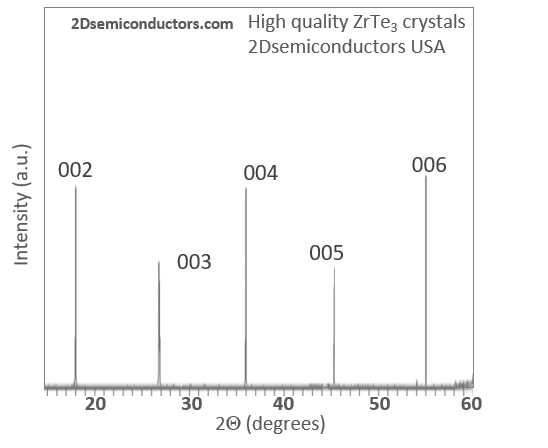


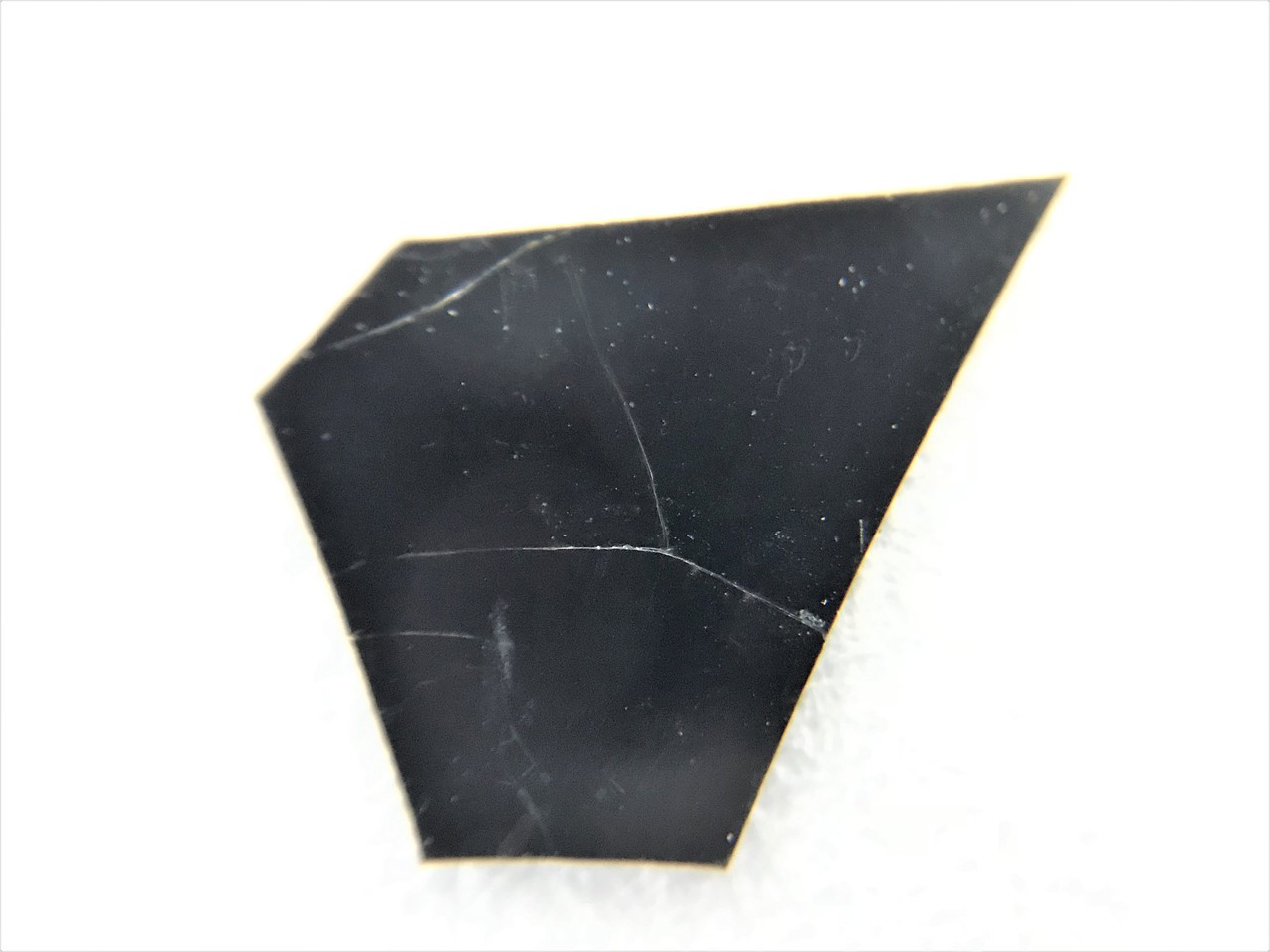
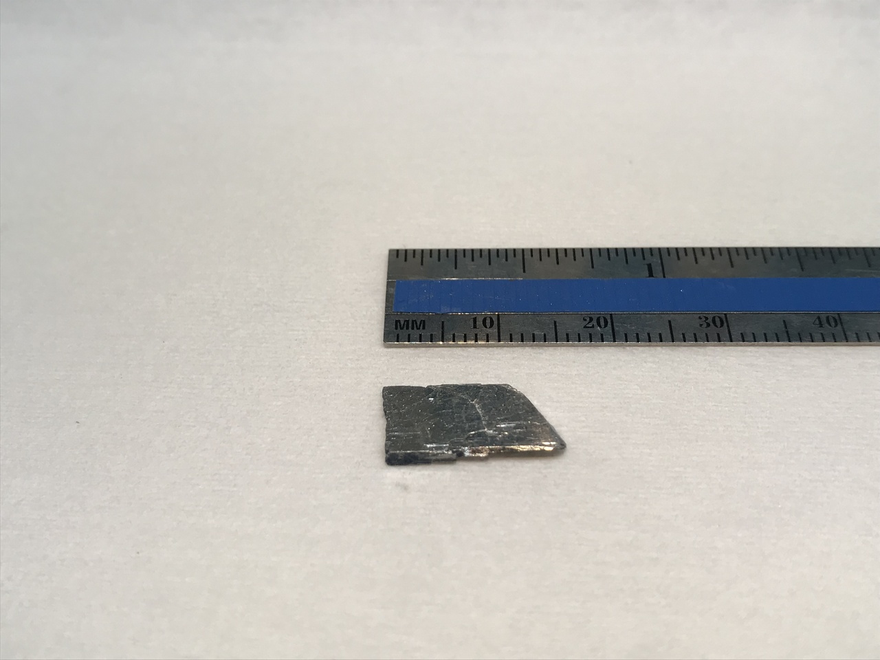
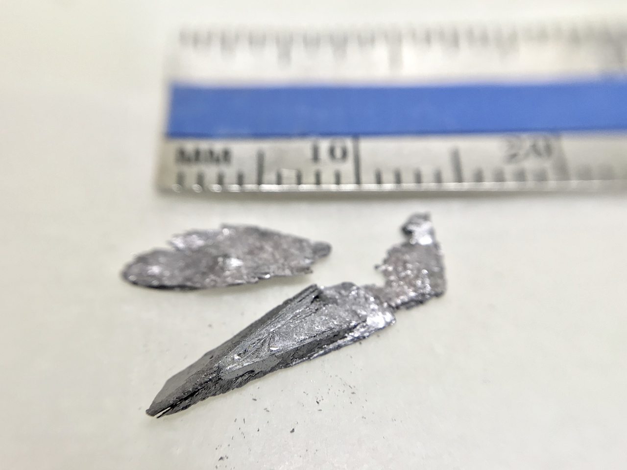
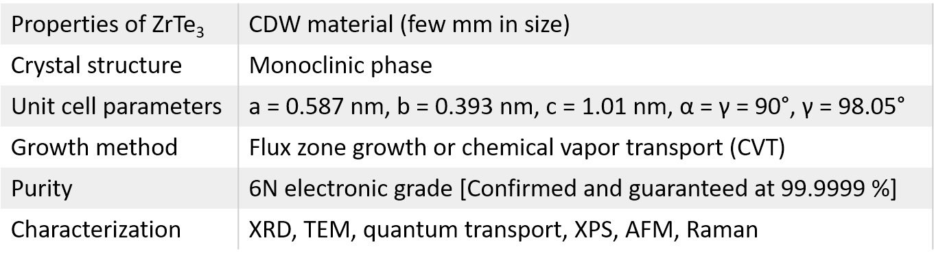
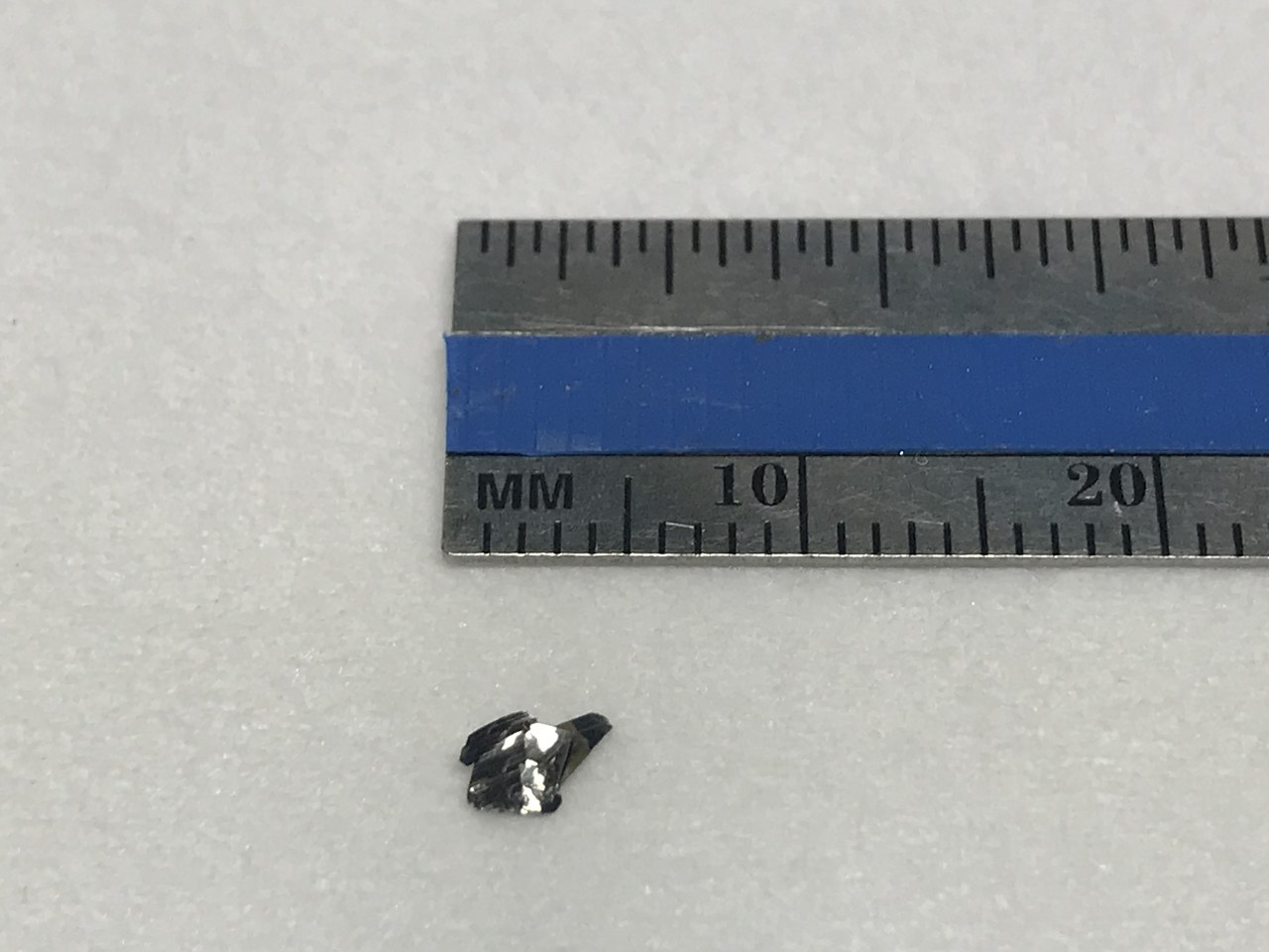
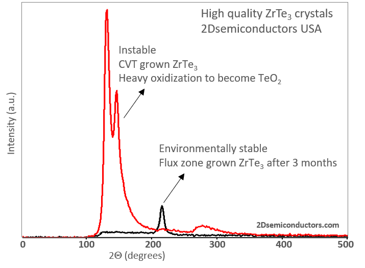
Zirconium Tritelluride belongs to the group-IV transition metal trichalcogenides. Unlike many ZrTe3 crystals, our crystals have been engineered to attain rather low record defect density (1E9-1E10cm-2) to yield environmentally stable ZrTe3 crystals. Please see Raman spectrum in this document; CVT grown crystals age in air rather quickly whereas flux grown crystals exhibit their true Raman signatures. In fact, Te defects are well-known cause for environmental degradation effects as well as reduced material quality and performace. Environmentally stable anisotropic transition metal trichalcogenide material ZrTe3 is available at 2Dsemiconductors USA. ZrTe3 crystals exhibit semimetallic behavior with charge density waves (CDW) phenomena at temperatures below ~70K. Material undergoes superconducting transition at ~2.7K in bulk but it is anticipated to have larger Tc for mono- and few-layers depending on the substrate monolayer interaction. The layers are stacked together via van der Waals interactions and can be exfoliated into thin 2D layers. Our crystals come with guaranteed CDW behavior and stability.
Growth method matters> Flux zone or CVT growth method? Contamination of halides and point defects in layered crystals are well known cause for their reduced electronic mobility, reduced anisotropic response, poor e-h recombination, low-PL emission, and lower optical absorption. Flux zone technique is a halide free technique used for synthesizing truly semiconductor grade vdW crystals. This method distinguishes itself from chemical vapor transport (CVT) technique in the following regard: CVT is a quick (~2 weeks) growth method but exhibits poor crystalline quality and the defect concentration reaches to 1E11 to 1E12 cm-2 range. In contrast, flux method takes long (~3 months) growth time, but ensures slow crystallization for perfect atomic structuring, and impurity free crystal growth with defect concentration as low as 1E9 - 1E10 cm-2. During check out just state which type of growth process is preferred. Unless otherwise stated, 2Dsemiconductors ships Flux zone crystals as a default choice.
Properties of CDW ZrTe3 crystals

Related literature
Single layer of MX3 (M = Ti, Zr; X = S, Se, Te): A new platform for nano-electronics and optics; Phys.Chem.Chem.Phys.,2015, 17, 18665
Angle resolved vibrational properties of anisotropic transition metal trichalcogenide nanosheets; Nanoscale, 2017,9, 4175-4182
聯(lián)系人:嚴(yán)春偉
手機:13914543285
電話:0523-86190619,86192878
郵箱:taizhou@sunano.com.cn
地址: 江蘇省泰州市鳳凰西路168號