歡迎光臨~泰州巨納新能源有限公司
語言選擇:
 ∷
∷

∷
 ∷
∷
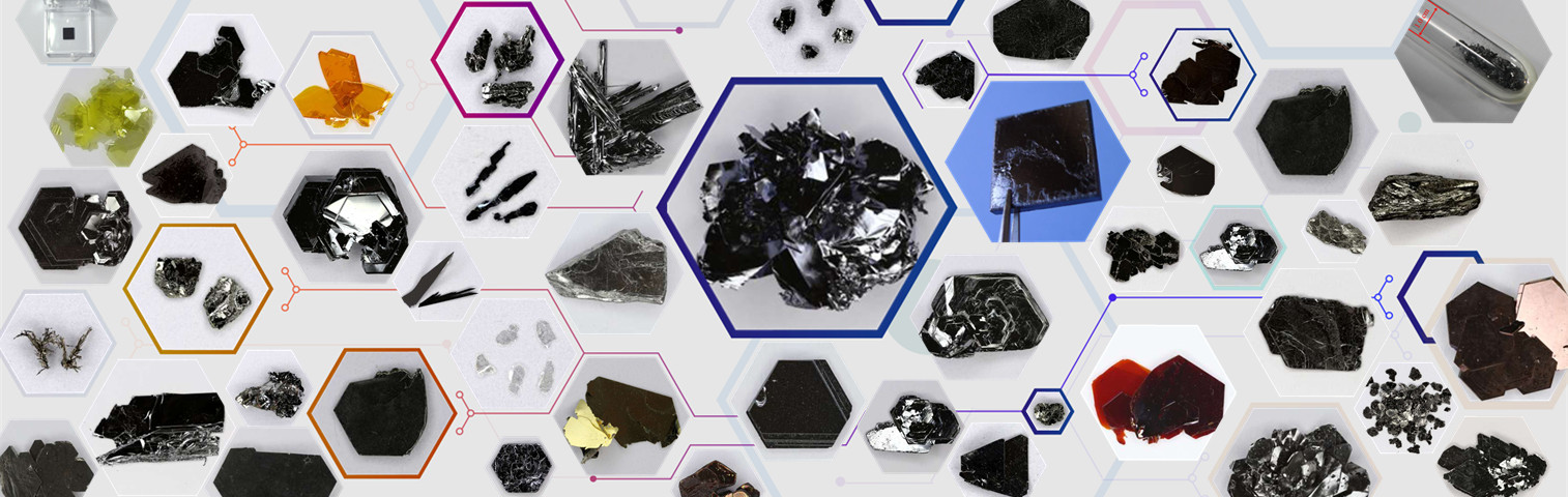
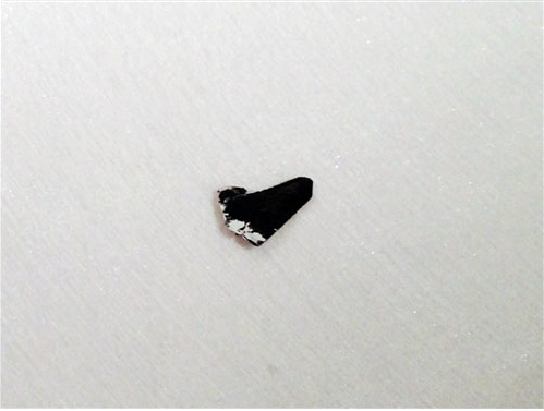
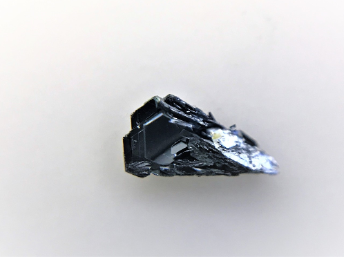
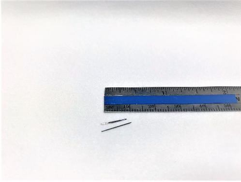
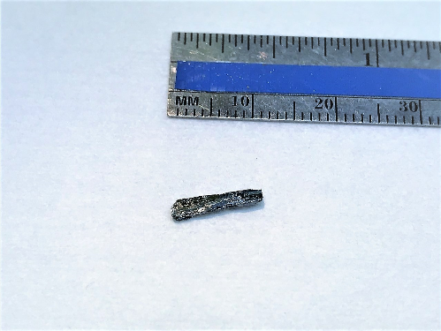
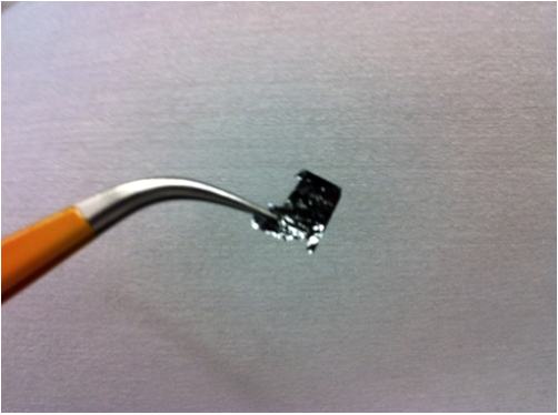
Similar to graphene and MoS?, VSe? is also layered material (layered transition metal dichalcogenide) crystallizing in the 1T-CdI2 structure. It is known to be a truly two-dimensional conductor (J. Phys. C: Solid State Phys. 17 2193) .Owing to weak interlayer couple can be isolated to monolayers on variety substrates. From few- to monolayers, VSe? possesses various interesting physical properties ranging from unusual - extraordinary Raman spectra and electrical conductivity. Each sample is characterized by various techniques such as electrical conductivity, Raman spectrum, XRD, XPS, AES, and ARPES to provide the highest quality samples for your research needs. Our single crystal VSe2 crystals come with guaranteed charge density wave (CDW) response.
Important characteristics of our VSe2 crystals
1. Environmental stability: We understand that defects actually cause these material to be unstable, and we specialize in lowering the defect density (using unique growth techniques) to create environmentally stable crystals
2. Stoichiometry: We sell 100% 1:2 stoichiometric ratios. They have exact stoichiometric value.
3. Defects: We are in business for more than 10 years and during these years, we have perfected our materials syshesis lines to achieve 1 out of 10000 site defect density or lower.
4. Grain size: Our grain size reaches really large and therefore you can get monolayers with 90% transfer rate (using our techniques) and get rather large areas (because single crystal grain size is large!).
5. Electronic and optical response: We characterize our samples usingstate of techniques to confirm excitonic dynamics (ultra fast spectroscopy), TEM, HRTEM, nano XPS and AES, SIMS (1ppm impurity resolution). We also make sure that residual resistance is minimized.
Growth method matters> Flux zone or CVT growth method? Contamination of halides and the presence point defects in layered crystals are well known cause for their weak CDW response, high electronic resistivity, and environmental instability. Flux zone technique is a halide free and slow growth technique used for synthesizing high-quality vdW crystals. This method distinguishes itself from chemical vapor transport (CVT) technique used by others in the following regard: CVT is a quick (~2 weeks) growth method but exhibits poor crystalline quality and the defect concentration reaches to 1E11 to 1E12 cm-2 range. In contrast, flux method takes long (~3 months) growth time, but ensures slow crystallization for perfect atomic structuring, and impurity free crystal growth with defect concentration as low as 1E9 - 1E10 cm-2.
During check out just state which type of growth process is preferred (CVT vs Flux zone). We recommend flux zone, and unless otherwise stated, 2Dsemiconductors ships Flux zone crystals as a default choice.
聯系人:嚴春偉
手機:13914543285
電話:0523-86190619,86192878
郵箱:taizhou@sunano.com.cn
地址: 江蘇省泰州市鳳凰西路168號