歡迎光臨~泰州巨納新能源有限公司
語言選擇:
 ∷
∷

∷
 ∷
∷
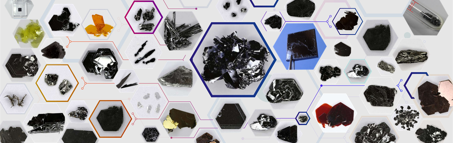

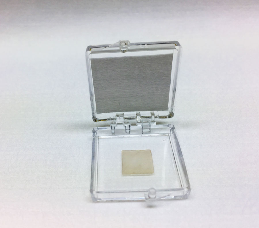
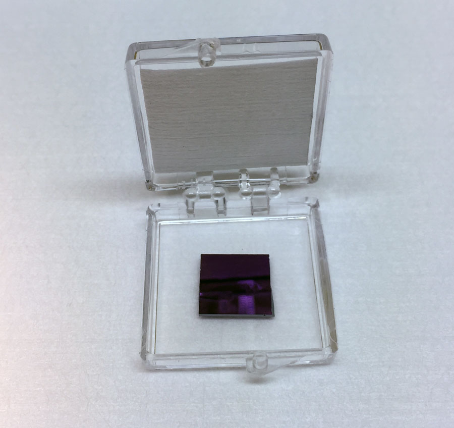
Substrate:
Sapphire (c-cut)
Quartz (Silica)
TEM grids (please supply grids)
Thermal Oxide (SiO2/Si)
Polyethylene terephthalate – PET Substrates
Pick your own substrates (please define the substrate type)
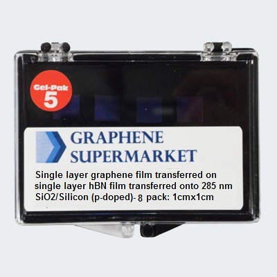
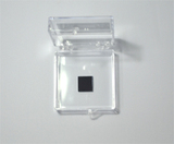
Our R&D has developed scalable methods to transfer 2D CVD grown sheets back to back to create 2D vertical heterojunctions. Even though 2D semiconductors R&D team uses chemical free transfer process, it is anticipated to observe transfer (strain, substrate, and defect) related changes in the physical properties of 2D layers. Because of the custom nature of the production process, all transferred CVD sales are final and non-refundable.
This product gives an idea about our capabilities on variety of substrates and heterojunction arrangements. The pricing largely dependents on the substrate types, CVD monolayers, and other technical challenges specific to your applications and sample specifications. Rule of thumb, you should expect the cost to be at least CVD costs (2 samples for 2 heterolayers). Our R&D works hard and is dedicated to creating your designer CVD products at affordable rates.
聯(lián)系人:嚴(yán)春偉
手機(jī):13914543285
電話:0523-86190619,86192878
郵箱:taizhou@sunano.com.cn
地址: 江蘇省泰州市鳳凰西路168號(hào)